|
Author: Dr Yu-Han Chang, Senior Technology Analyst at IDTechEx Semiconductor packaging technologies have evolved from initial 1D PCB levels to the cutting-edge 3D hybrid bonding packaging at the wafer level. This advancement facilitates single-digit micronmeter interconnecting pitches, achieving over 1000 GB/s bandwidth with high energy efficiency. Four critical parameters shape advanced semiconductor packaging: power, performance, area, and cost:
2.5D and 3D packaging technology:
|
||

|
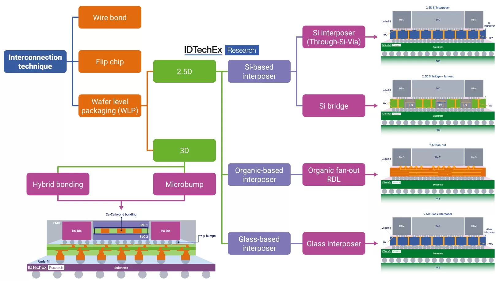
Overview of advanced semiconductor packaging technologies. Source: IDTechEx – “Advanced Semiconductor Packaging 2024-2034: Forecasts, Technologies, Applications” |
||
|
The 2.5D and 3D packaging technologies encompass various packaging techniques. In 2.5D packaging, the choice of interposer material categorizes it into Si-based, Organic-based, and glass-based interposers, as illustrated in the figure above. Meanwhile, in 3D packaging, the evolution of microbump technology aims for smaller pitch dimensions. However, achieving single-digit pitch dimensions today is made possible through the adoption of hybrid bonding technology, a method that directly connects Cu-Cu, signifying a significant advancement in the field. Advantages and drawbacks of each packaging type in both 2.5D and 3D configurations 2.5D Si: There are two alternatives within this category: Si interposer, utilizing a full passive Si wafer, and Si bridge, which can take the form of a localized Si bridge in a fan-out based molding compound or in a substrate with a cavity. The Si interposer, commonly employed in 2.5D packaging for high-performance computing integration due to its ability to facilitate the finest routing features, faces challenges associated with its cost in both materials and manufacturing compared to alternatives like organic materials, and the packaging area limitation. To address this, the localized Si bridge form is gaining prominence, strategically utilizing Si where fine features are essential. Additionally, the Si bridge structure is expected to see increased use, particularly in scenarios where Si interposer faces limitations in area, pushing beyond the 4x or 5x reticle limit. Organic: In the report, we specifically consider organic-based packaging that utilizes a fan-out molding compound rather than an organic substrate. Organic materials, with the capability to adjust their dielectric constant lower than silicon, contribute to lower RC delay in the package. Moreover, these materials present a more cost-effective alternative to silicon. These advantages drive the emergence of organic-based 2.5D packaging. However, a key drawback lies in the challenges associated with achieving the same level of interconnect feature reduction as Si-based packages. Glass: The glass-based approach has gained significant interest following Intel's unveiling of its glass-based test vehicle package earlier this year. Glass possesses advantageous properties, including tunable Coefficient of Thermal Expansion (CTE), high dimensional stability, and a smooth, flat surface. These characteristics position glass as a promising candidate for serving as an interposer, with routing features that have the potential to rival those offered by silicon. However, the main drawback of glass lies in its immature ecosystem and a current lack of large-volume mass production capability in the packaging industry. Nevertheless, as the ecosystem matures and production capabilities advance, the use of glass-based technologies in semiconductor packaging may see further growth. 3D Microbump: The well-established microbump technology, based on the Thermal Compression Bonding (TCB) process, has a longstanding presence across diverse products. Its roadmap involves ongoing scaling of bumping pitch. However, a critical challenge emerges as smaller solder ball sizes in this process result in heightened Intermetallic Compounds (IMCs) formation, diminishing conductivity and mechanical properties. Additionally, close contact gaps may lead to solder ball bridging, risking chip failure during reflow. With solder and IMCs exhibiting higher resistivity than copper, their use in high-performance component packaging faces limitations. Hybrid bonding: Hybrid bonding involves creating permanent interconnections by combining a dielectric material (SiO2) with embedded metal (Cu). With Cu-Cu hybrid bonding achieving pitches below 10 micrometers (typically around one-digit µm), advantages include expanded I/O, increased bandwidth, enhanced 3D vertical stacking, heightened power efficiency, and reduced parasitics and thermal resistance due to the absence of underfill. Challenges encompass manufacturing complexities and higher costs associated with this advanced technique. IDTechEx’s new report, “Advanced Semiconductor Packaging 2024-2034: Forecasts, Technologies, Applications“, thoroughly explores the latest innovations in semiconductor packaging technology, covering key technical trends, analyzing the value chain, evaluating major players, and providing detailed market forecasts. The report recognizes the crucial role of advanced semiconductor packaging as the foundation for next-generation ICs. It focuses on its applications in key markets such as AI and data centers, 5G, autonomous vehicles, and consumer electronics. Leveraging IDTechEx's expertise in these sectors, the report delivers a comprehensive understanding of the impact and future trajectory of advanced semiconductor packaging in these critical fields. Key aspects of this report: Exploring Technology Trends and Manufacturers in Advanced Semiconductor Packaging:
10-year Granular Market Forecasts & Analysis:
To find out more about this new IDTechEx report, including downloadable sample pages, please visit www.IDTechEx.com/ASP. Free-to-attend upcoming webinar Advancement in 2.5D and 3D Semiconductor Packaging Technologies Dr Yu-Han Chang, Senior Technology Analyst at IDTechEx and author of this article, will be presenting a free-to-attend webinar on the topic on Wednesday 17 January 2024 – Advancement in 2.5D and 3D Semiconductor Packaging Technologies. This webinar will reveal insights into 2.5D and 3D advanced semiconductor packaging technologies and the content include:
Click here to find out more and register your place on one of our three sessions. If you are unable to make the date, please register anyway to receive the links to the on-demand recording (available for a limited time) and webinar slides as soon as they are available. |

